TFLN Photonic Chip Foundry
Accelerate the development of your integrated photonic circuits on Thin-Film Lithium Niobate (TFLN) with our foundry services.

INO offers its foundry services to technology companies, universities, and other organizations. Its TFLN (Thin-Film Lithium Niobate) integrated photonic chip platform combines advanced microfabrication, R&D flexibility, and recognized expertise in microsystem integration.
A TFLN Platform to Turn Your Designs into Functional Photonic Circuits
Access Modes to the TFLN Foundry
Initial PDK available through private projects.
- MPW (Multi-Project Wafer)
Shared access to the TFLN platform. - Proprietary Short-Run Production
R&D partnership for proprietary short-run manufacturing. - À la Carte Services
TFLN etching, microfabrication, optical and electrical characterization, and packaging.
INO continuously develops its TFLN PIC platform to deliver an integrated value chain covering design, fabrication, testing, and packaging of integrated photonic circuits.
Our Ambition
Supporting our clients in transforming their photonic concepts and designs into functional, tested circuits by combining:
Expertise
Flexibility
Collaboration
Overview of Our Key Technical Capabilities

840 m² of cleanroom facilities

35 years of experience

Advanced process expertise

Wafer-level and die-level testing
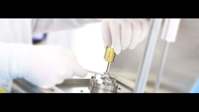
Heterogeneous, hermetic, and vacuum packaging capabilities
typical Applications
INO’s microfabrication services are intended for, but not limited to, the following sectors:
- Telecommunications and datacom
- Artificial intelligence and photonic computing
- Space
- Quantum technologies
- Biomedical technologies
- Research and development
- Emerging photonic applications
Example Use Cases
INO’s microfabrication services are well suited for, among others:
Integrated photonic modules
Advanced optical microsystems
Why Choose INO?
- Dedicated TFLN platform for integrated photonic circuits
- Processing of 100, 150, and 200 mm wafers
- ISO Class 100, 1,000, and 10,000 cleanrooms
- Heterogeneous, hermetic, and vacuum packaging, including optical alignment
- Flexible and fast R&D approach: prototyping, short-run production, MPW
- Network of specialized technology partners
- Proven experience with major players in the telecom, datacom, and quantum sectors
- Ability to collaborate with fabless companies, start-ups, and universities
- Canada’s only TFLN foundry, offering a strategic local footprint
- Certifications: ISO 9001, ISO 14644-1, and ESD ANSI S20.20
Compliance with PMC/CGP, ESA ECSS, and ISO 13485 available as required - Expertise in monolithic fabrication on CMOS wafers
INO, founding Partner of FABrIC
INO, together with Aeponyx, EXFO, and C2MI, is among the beneficiaries of the FABrIC program—a major initiative managed by CMC Microsystems and funded by the government of Canada, aimed at strengthening Canada’s capabilities in semiconductor design, prototyping, and manufacturing across strategic technologies including photonics, MEMS, quantum, and compound semiconductors.